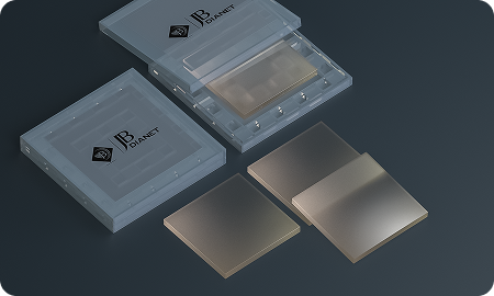
Our Products
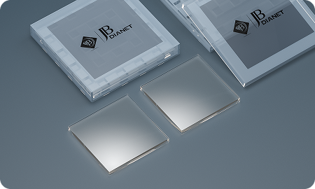
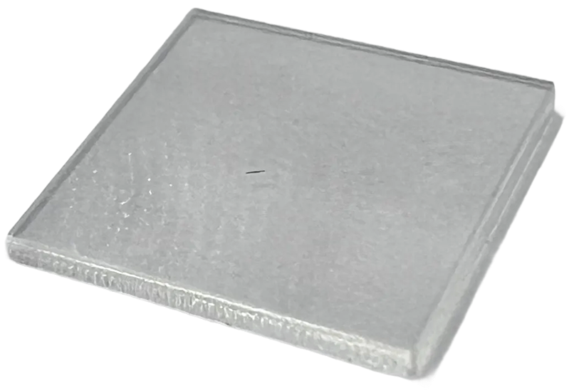
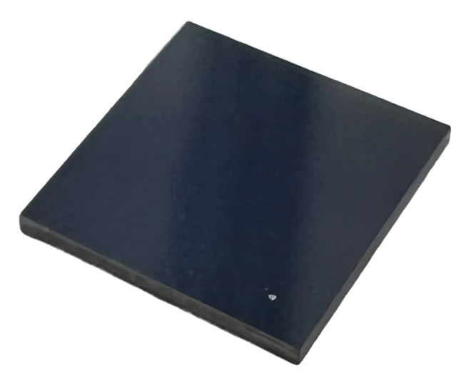
Single Crystal CVD Diamond Plate
Product Description
Single-crystal CVD diamond plates offer superior thermal conductivity (up to 2200 W/m·K), making them ideal for heat dissipation in high-power electronics, lasers, RF devices, and semiconductors.
Size : 2mm to 20mm
Specifications and Tolerances
 Edges: Laser Cut
- Face / Surface Orientation: 100
- Laser Kerf: 3°
- Lateral Tolerance: +0.2/-0 mm
- Side 1, Roughness, Ra: polished,
Ra
< 2 - 30 nm
- Side 2, Roughness, Ra: polished,
Ra
< 2 - 30 nm
- Thickness Tolerance: +/- 0.05 mm
- Thickness Dimension: 0.3-0.5mm
Material Properties
- Nitrogen concentration: < 5 ppb ( Optional
) N2 Controlled based on Requirements
Advantage
- Exceptional thermal
conductivity : Higher than polycrystalline, offering superior heat
dissipation.
- Isotropic properties :
Uniform thermal performance in all directions, ideal for precision applications.
- High thermal stability :
Performs well at extreme temperatures without degradation.
- Electrical insulation :
Non-conductive, useful in electronic devices requiring thermal control without
affecting electrical circuits.
- Minimal defects : Ensures
higher reliability and efficiency in sensitive thermal management systems.
- Durability: Resistant to
wear
and chemical exposure, prolonging lifespan in demanding environments.
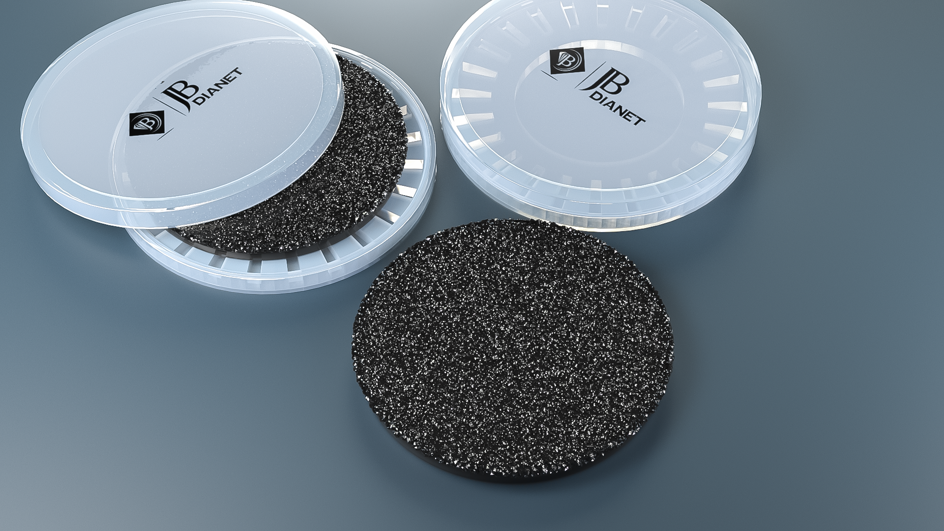
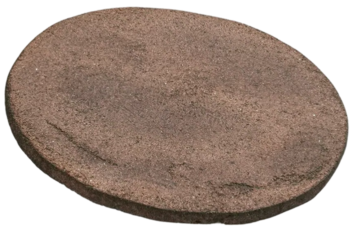
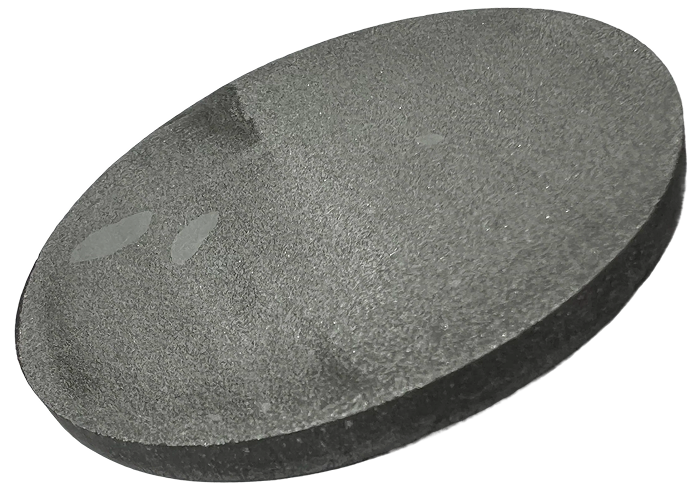
PolyCrystal CVD Diamond Wafer
Product Description
Polycrystalline CVD diamond (PCD) plates provide excellent thermal management with high thermal conductivity, though slightly lower than single-crystal diamonds. They are ideal for use in heat sinks and spreaders in electronics, RF devices, and power systems, offering efficient heat dissipation and enhanced durability, which helps improve the longevity and reliability of electronic components in demanding environments.
Specifications and Tolerances
 Diameter: 10 mm to 100 mm
- Thickness: 300um & 500um
- Thermal conductivity: Up To
1800
W/mK
- Surface : As grown & polished
one
/two side with 20nm
- Thickness Tolerance : +/- 5%
- Transmittance : up to 65%
Advantage
- High thermal
conductivity
:
Superior heat dissipation, ideal for high-power electronics.
- Low thermal
expansion :
Reduces stress between materials during temperature changes.
- Chemical stability :
Resistant to oxidation and chemical reactions at high temperatures.
- Wear resistance :
Ensures
durability and long-lasting performance in harsh environments.
- Radiation resistance
:
Suitable for space and high-radiation environments.
- Electrical
insulation :
Useful in applications requiring thermal management without electrical conductivity.
Ultra-High Purity 30 to 50 μm Epi Layer on SCD
Size – 5mm to 20mm
Specifications and Tolerances
- Boron
concentration: < 5 ppb
- Surface
roughness: < 2 nm
- Nitrogen
concentration: < 5 ppb
- Orientation:
Typically (100)
Applications
-
High-frequency and high-power
electronic devices
- Optical
windows with ultra-low
absorption
- Quantum
optics: NV⁰ and NV⁻ centre
stability
-
Ultrafast photodetectors
Industries
- Quantum
Photonics
- Laser &
LIDAR Systems
-
High-Frequency RF/Power Electronics
- Advanced
Sensor Technologies
Cu-Diamond Composite Material
Specifications and Tolerances
- Thermal
conductivity: 500–700
W/m·K
- CTE
tailored to match Si or GaN
- Thickness:
0.5 mm – 5 mm or as
per customised design
- Surface:
Lapped, Laser Cut
Applications
-
High-power RF amplifier
baseplates
-
Space-grade thermal
interface materials
-
IGBT module heat sinks
-
LED packaging
Industries
-
Power Electronics
-
Satellite and Defense
Avionics
-
Automotive EV Modules
-
LED Packaging
Boron Doped SCD Diamond
Size : 2mm to 20mm
Specifications and Tolerances
-
Thickness: 0.3 mm – 1 mm
- Boron
concentration:
1017–1021 atoms/cm3
-
Orientation: (100)
-
Electrical conductivity: from
semiconductor to metallic behaviour
-
Resistivity: ~1 mΩ·cm (highly
doped)
- Surface
roughness: Polished up to
2nm
Applications
-
Electrochemical sensors and
electrodes
-
Radiation-hardened electronics
- p-type
semiconductor devices
Industries
-
Harsh-Environment Electronics
(space, nuclear)
-
Diamond-based Transistors
-
Electrochemical Sensing
Aluminium-Diamond Composite Plates
Specifications and Tolerances
-
Diamond volume fraction:
30–50%
-
Thermal conductivity: 350–500
W/m·K
-
CTE matched with Si or GaAs
-
Surface treatment: Lapped,
Laser Cut
-
Thickness: 0.3 mm – 10 mm or
as per customised design
Applications
-
Heat spreaders in telecom and
radar
-
Optoelectronic devices
thermal management
-
Laser diode mounting
-
LED arrays
Industries
-
Telecom Infrastructure
-
Medical Lasers
-
Consumer Electronics
-
Aerospace Electronics
GaN on Diamond
Specifications and Tolerances
- GaN
thickness: 0.5 μm – 5 μm
-
Substrate: SCD (100) or (111),
polished
-
Interface: Buffer layer (e.g., AlN
or AlGaN)
-
Crystalline quality: Low
dislocation density
- Thermal
resistance: Ultra-low (< 0.1 K/W)
Applications
- GaN
HEMTs with high power density
- Next-gen
radar and communication
systems
- RF and
5G devices
- Thermal
management-critical devices
Industries
- Wireless
Communications
- 5G
Infrastructure
- Military
Radar
-
High-Power Electronics
GaN Bonded on PCD Wafer (4-inch)
Specifications and Tolerances
-
PCD wafer: 2-4 inch, 300–500
μm thick
-
GaN layer: Transferred or
bonded
-
Bonding method:
Plasma-assisted
-
Interface thermal resistance:
Minimized for high-power use
Applications
-
GaN-on-Diamond HEMTs
-
GaN LEDs with enhanced heat
dissipation
-
Pulsed RF Power Amplifiers
-
Monolithic microwave
integrated circuits (MMICs)
Industries
- RF
& Microwave
-
High-Speed Switching Systems
-
Space-grade Electronics
-
Defence Electronics